
Feature
- Up to 5 samples, which can be measured automatically
- Analysis software with easy operation
- The control freely depth observation
- Measured pore size is atomic-vacancy from 10nm
- Low-damage, non-destructive
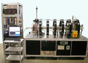
Specification and Performance
- Space occupied by the equipment:4.7mx3.2mx2.2m(H)
- Positron source:Na-22 (max.activity 1GBq)
- Positron beam energy:0.5~15keV(variable)
- Time resolution:<300ps
- γ-ray counting rate:>500cps@1GBq
- Measurement time:<1h/spectrum
Application
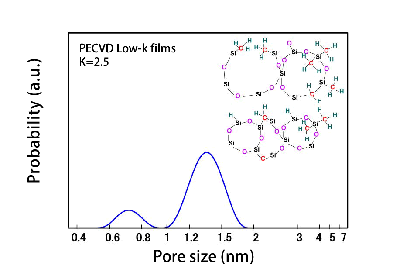
- VLSI materials:
Low-k dielectrics, High-k gate dielectrics, Cu barrier films, Electroplated Cu films, SIO, Strained Si, Ion-implanted Si - Ⅲ-Ⅴ, Ⅱ-Ⅵ semiconductors:
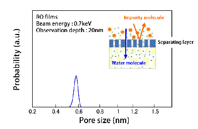
GaN, InN, ZnO, SiC, GaAs - Porous materials, Zeolite, Membranes, Polymer coating films (free volume)
RO films, Gas barrier films,
Mesoporous materials
Designed and developed by
Advanced Defect-Characterization Research Group, Research Institute of Instrumentation Frontier, National Institute of Advanced Industrial Science and Technology (AIST)